


The global Wafer Bonding Equipment market was valued at USD 333.38 million in 2023 and is projected to reach USD 568.81 million by 2033, at a CAGR of 5.5% during the forecast period 2024-2033.
Introduction
The wafer bonding equipment market plays a critical role in semiconductor manufacturing, facilitating the integration of various materials and structures on semiconductor wafers. This technology is essential for producing advanced electronic components, including microelectromechanical systems (MEMS), 3D integrated circuits (ICs), and various optoelectronic devices. As the demand for smaller, more efficient, and higher-performance electronic devices grows, the wafer bonding equipment market is experiencing significant expansion and innovation.
Definition and Working Principle
Definition: Wafer bonding is a process that joins two semiconductor wafers or a wafer and a substrate to create a single, cohesive unit. This process is integral in fabricating multi-layered semiconductor devices, enabling the creation of complex architectures and enhancing device performance.
Working Principle: Wafer bonding involves aligning and bonding two or more wafers using various techniques, such as thermal compression, anodic bonding, or adhesive bonding. The bonded wafers undergo further processing to form integrated circuits or MEMS devices. Key steps include surface preparation, alignment, bonding, and annealing to achieve a strong and reliable bond.
Historical Context and Evolution
Early Developments:
- 1950s-1960s: Initial experiments in wafer bonding focused on basic adhesion techniques for simple device fabrication.
- 1970s: Development of anodic bonding, primarily used for glass-silicon interfaces, revolutionized MEMS production.
Technological Advancements:
- 1980s-1990s: Introduction of fusion bonding and improved alignment systems enabled more complex device integration, facilitating advancements in MEMS and ICs.
- 2000s-Present: Emergence of advanced techniques like wafer-level bonding and hybrid bonding has driven significant improvements in performance, miniaturization, and integration capabilities.
Key Milestones:
- Development of SOI (Silicon-on-Insulator): Pioneered the use of wafer bonding for fabricating high-performance microelectronics.
- Advancements in MEMS Fabrication: Enabled the creation of sophisticated sensors and actuators for automotive, consumer electronics, and medical applications.
- Integration of 3D ICs: Pushed the boundaries of wafer bonding by facilitating vertical integration and enhancing computational capabilities in smaller form factors.
Market Dynamics
Market Drivers:
- Increasing Demand for Miniaturization: The ongoing trend towards smaller, more powerful electronic devices drives the demand for advanced wafer bonding technologies capable of supporting high-density integration.
- Growth in MEMS and Sensors: Expanding applications in automotive, healthcare, and consumer electronics fuel the demand for wafer bonding equipment to produce high-precision MEMS devices.
- Advancements in 3D ICs: The push towards 3D integration in semiconductor devices requires reliable wafer bonding solutions to achieve high performance and efficiency in compact designs.
Market Restraints:
- High Capital Costs: The significant investment required for wafer bonding equipment and technology development can be a barrier for new entrants and small-scale manufacturers.
- Technical Challenges: Issues related to alignment accuracy, bonding strength, and material compatibility pose ongoing challenges in wafer bonding processes.
Market Opportunities:
- Emergence of Advanced Packaging Technologies: Innovations in advanced packaging, such as fan-out wafer-level packaging (FOWLP) and system-in-package (SiP), offer new growth opportunities for wafer bonding equipment.
- Expanding Applications in IoT and AI: The proliferation of Internet of Things (IoT) devices and artificial intelligence (AI) applications creates a growing need for sophisticated wafer bonding solutions to support diverse functionalities and connectivity.
Technological Innovations
Emerging Technologies:
- Hybrid Bonding: Combines the benefits of adhesive and fusion bonding to achieve high bond strength and reliability with improved alignment accuracy.
- Wafer-Level Bonding: Enables bonding at the wafer level rather than individual die level, improving throughput and reducing costs in high-volume production.
- Plasma-Assisted Bonding: Utilizes plasma treatment to enhance surface activation and bonding strength, particularly useful for challenging material combinations.
Material Innovations:
- Advanced Adhesives: Development of high-performance adhesives that offer improved thermal and mechanical properties for diverse applications.
- New Substrates: Exploration of novel substrates such as glass and advanced ceramics for specialized applications, enhancing compatibility and performance.
Automation and Integration:
- Automated Alignment Systems: Integration of high-precision alignment systems with wafer bonding equipment to enhance accuracy and throughput.
- Integrated Metrology: Incorporation of metrology tools for real-time monitoring and quality control during the bonding process, improving yield and reducing defects.
Future Outlook
Market Projections:
- Growth Forecast: The global wafer bonding equipment market is expected to grow at a compound annual growth rate (CAGR) of 8-10% from 2024 to 2030, driven by advancements in semiconductor manufacturing and increasing demand for miniaturized electronic devices.
- Technological Trends: Continued innovation in bonding techniques, automation, and material science will drive market growth and enable the development of next-generation semiconductor devices.
- Regional Trends: North America and Asia-Pacific are expected to lead in market growth, with significant contributions from semiconductor manufacturing and technology development.
Key Developments to Watch:
- Emergence of New Bonding Techniques: Ongoing research into hybrid bonding, plasma-assisted bonding, and other advanced techniques will shape the future of wafer bonding technology.
- Integration with Emerging Technologies: The integration of wafer bonding with emerging technologies such as quantum computing, advanced sensors, and flexible electronics will open new markets and applications.
- Focus on Sustainability: Increasing emphasis on sustainable manufacturing practices will drive the development of eco-friendly bonding solutions and processes.
Receive the FREE Sample Report of Wafer Bonding Equipment Market Research Insights @ https://stringentdatalytics.com/sample-request/wafer-bonding-equipment-market/9687/
Market Segmentations:
Global Wafer Bonding Equipment Market: By Company
• EV Group
• SUSS MicroTec
• Tokyo Electron
• Applied Microengineering
• Nidec Machinetool
• Ayumi Industry
• Shanghai Micro Electronics
• U-Precision Tech
• Hutem
• Canon
• Bondtech
• TAZMO
• TOK
Global Wafer Bonding Equipment Market: By Type
• Fully Automatic
• Semi Automatic
Global Wafer Bonding Equipment Market: By Application
• MEMS
• Advanced Packaging
• CIS
• Others
Regional Analysis of Global Wafer Bonding Equipment Market
All the regional segmentation has been studied based on recent and future trends, and the market is forecasted throughout the prediction period. The countries covered in the regional analysis of the Global Wafer Bonding Equipment market report are U.S., Canada, and Mexico in North America, Germany, France, U.K., Russia, Italy, Spain, Turkey, Netherlands, Switzerland, Belgium, and Rest of Europe in Europe, Singapore, Malaysia, Australia, Thailand, Indonesia, Philippines, China, Japan, India, South Korea, Rest of Asia-Pacific (APAC) in the Asia-Pacific (APAC), Saudi Arabia, U.A.E, South Africa, Egypt, Israel, Rest of Middle East and Africa (MEA) as a part of Middle East and Africa (MEA), and Argentina, Brazil, and Rest of South America as part of South America.
Click to Purchase Wafer Bonding Equipment Market Research Report @ https://stringentdatalytics.com/purchase/wafer-bonding-equipment-market/9687/
Regional Insights
North America:
- Market Characteristics: Dominated by advanced semiconductor manufacturing and strong presence of leading technology companies.
- Growth Drivers: High investment in research and development, demand for advanced consumer electronics, and expansion of IoT and AI applications.
Europe:
- Market Characteristics: Focus on automotive and industrial applications, with significant contributions from MEMS and sensor technologies.
- Growth Drivers: Increasing integration of electronics in automotive systems, growing demand for industrial automation, and support for renewable energy technologies.
Asia-Pacific:
- Market Characteristics: Rapidly growing semiconductor manufacturing hub with high demand for consumer electronics and automotive applications.
- Growth Drivers: Expansion of manufacturing capacities, growing adoption of advanced packaging technologies, and increasing investments in semiconductor R&D.
Rest of the World:
- Market Characteristics: Emerging markets with growing interest in semiconductor manufacturing and applications in various industries.
- Growth Drivers: Investment in technology infrastructure, demand for advanced electronic devices, and development of regional semiconductor ecosystems.
Competitive Landscape
Key Players:
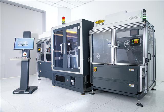
- EV Group (EVG): Known for its comprehensive range of wafer bonding solutions, including fusion, anodic, and hybrid bonding systems.
- SUSS MicroTec: Offers advanced wafer bonding equipment for MEMS, sensors, and advanced packaging applications.
- Tokyo Electron Limited (TEL): Provides high-precision wafer bonding equipment for semiconductor manufacturing, focusing on innovation and quality.
- Lam Research Corporation: Develops advanced bonding solutions integrated with etching and deposition technologies for comprehensive semiconductor fabrication.
Competitive Strategies:
- Innovation and R&D: Companies are investing heavily in research and development to innovate new bonding techniques and improve existing technologies.
- Strategic Partnerships: Collaborations with semiconductor manufacturers, research institutions, and technology providers to enhance product offerings and expand market reach.
- Expansion and Diversification: Expanding product portfolios to include a wider range of bonding solutions and entering new geographical markets to capture emerging opportunities.
Market Trends
Shift Towards 3D Integration:
- Overview: Increasing focus on 3D integration in semiconductor devices to enhance performance, reduce power consumption, and enable compact designs.
- Impact: Drives demand for advanced wafer bonding equipment capable of supporting high-precision and reliable bonding in 3D IC fabrication.
Adoption of Advanced Packaging Technologies:
- Overview: Growing adoption of advanced packaging solutions such as FOWLP and SiP to achieve higher integration density and improved performance.
- Impact: Fuels demand for wafer bonding equipment that can handle complex packaging requirements and support high-volume production.
Emphasis on Automation and Quality Control:
- Overview: Increasing emphasis on automation and real-time quality control in wafer bonding processes to enhance productivity and yield.
- Impact: Leads to the integration of advanced alignment systems, metrology tools, and automation technologies in wafer bonding equipment.
Focus on Energy Efficiency and Sustainability:
- Overview: Growing awareness of energy efficiency and sustainability in semiconductor manufacturing drives the development of eco-friendly bonding solutions.
- Impact: Promotes the adoption of energy-efficient equipment, advanced materials, and processes that minimize environmental impact.
Challenges and Opportunities
Challenges:
- Technical Complexity: Ensuring high alignment accuracy, bonding strength, and material compatibility remains a significant challenge in wafer bonding processes.
- Cost Pressures: Balancing the high costs of wafer bonding equipment and technology development with the need for cost-effective solutions in a competitive market.
- Regulatory Compliance: Meeting various international standards and regulations for semiconductor manufacturing and device safety.
Opportunities:
- Emerging Applications: Expanding applications in IoT, AI, and advanced packaging technologies offer new growth opportunities for wafer bonding equipment.
- Technological Advancements: Innovations in bonding techniques, materials, and automation technologies present opportunities for market differentiation and leadership.
- Expansion in Emerging Markets: Growing interest in semiconductor manufacturing and technology development in emerging markets creates new avenues for market expansion.
About Stringent Datalytics
Stringent Datalytics offers both custom and syndicated market research reports. Custom market research reports are tailored to a specific client’s needs and requirements. These reports provide unique insights into a particular industry or market segment and can help businesses make informed decisions about their strategies and operations.
Syndicated market research reports, on the other hand, are pre-existing reports that are available for purchase by multiple clients. These reports are often produced on a regular basis, such as annually or quarterly, and cover a broad range of industries and market segments. Syndicated reports provide clients with insights into industry trends, market sizes, and competitive landscapes. By offering both custom and syndicated reports, Stringent Datalytics can provide clients with a range of market research solutions that can be customized to their specific needs.
Reach US
Stringent Datalytics
+1 346 666 6655
Social Channels:
Leave a Reply